Lab 1: Building A Basic SoC
Description
In laboratory 1 you will complete a provided boilerplate design of a System-on-Chip (SoC) using the Xilinx-Vivado development suite and targeted at the Arty-A7-35 development board. Your design will contain a MicroBlaze soft processor, a USB UART serial controller, and a DDR memory controller that interfaces with components on the Arty board. The processor will be connected to the serial port and DDR memory peripherals in a shared-bus architecture. You will then program this SoC using the C programming language to print out your name and student ID five times to the screen of a desktop computer which is connected to the Arty-7 development board using the USB serial port. There will be 2 screenshot requirements for your report, so ensure you read the following instructions carefully.
Project Assignment
Use the provided base project to create a basic system-on-chip and add a UART serial controller to your SoC. Synthesize your system-on-chip, compile your software project, combine them into a bitstream, and download it onto the Arty-A7-35 development board. Create a software project and make it print out your name five times.
This may not seem like much, but at the end of this laboratory, you will have created a system-on-chip and executed a program on top of it in a bare metal environment. This represents a rudimentary but fully functional embedded system.
Directions
Preamble - Adding Arty board to Vivado:
Before opening Vivado, visit Digilent’s website and follow the instructions listed under “Install Digilent’s Board Files”. The instructions will provide you with a download link for the board files. When you extract the archive, you only need to install the “arty-a7-35” directory, other boards are not necessary for our purposes.
Vivado - Generating a bitstream:
- Start by downloading the base SoC project from GitHub.
- NB: Windows users - Extract the downloaded files to a directory close to your system root directory. E.g.
C:\Users\[username]\Desktop\eecs-4114-labs. Visit this page for Windows path character limit details.
- NB: Windows users - Extract the downloaded files to a directory close to your system root directory. E.g.
- Open the downloaded project in Vivado 2019.1.
- Option 1: In the project folder (e.g.
C:\Users\[username]\Desktop\eecs-4114-labs\base-soc), double-click the file base-soc.xpr - Option 2: Start by opening Vivado 2019.1. On the welcome screen, select “Open Project”. Use the dialog to navigate to your project directory, and open the base-soc.xpr file.
- Option 1: In the project folder (e.g.
- In the left panel, “Flow Navigator”, select the “Open Block Design” option.
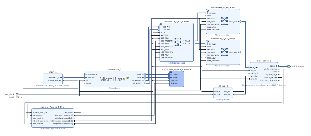
 PDF Version: Block Design
 - Add the AXI UARTlite soft-ip core to the design.
- Right-click anywhere in the board design window and select “+ Add IP…”.
- Enter “Uartlite” in the search window and double-click on the “AXI Uartlite” option. The AXI Uartlite soft-ip core should appear in the block design along with a green bar at the top of the window.
- In the green bar, select “Run Connection Automation”. Then, in the “Run Connection Automation” window, check the “UART” checkbox under “axi_uartlite..” and click “OK”. Important: leave the S_AXI box unchecked.
- Almost there… Right-click the S_AXI port on the AXI Uartlite core and select “Make Connection…”. In the “Make Connection” window, select the M00_AXI under microblaze_0_axi_periph and click “OK” to make the connection.
- Finally, select “Run Connection Automation” again. Select s_axi_clk under axi_uartlite.. and change the “Clock Source:” option to
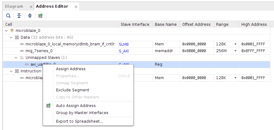
/mig_7series_0/ui_clk (81 MHz). Click “OK” to automate the connection of the clock and reset ports. - You may need to assign an address to the AXI Uartlite soft-ip. Open the “Address Editor” window and verify that an address has been assigned to “axi_uartlite..”. If not, right-click on “axi_uartlite..” and select “Auto Assign Address”.

- In the “Sources” window, right-click on the “base_soc.bd” file and select “Create HDL Wrapper…”. The “base_soc.bd” file should now be nested inside “base_soc_wrapper.v” file.
- Back in the “Flow Navigator” window, select “Generate Bitstream” to synthesize your design. This may take a while…
- After generating a bitstream, select
File > Export > Export Hardwarein the top menu. Then in the export window, select the “Include bitstream” option before exporting your design.
SDK - Creating Software Project:
- To open the SDK environment, select
File > Launch SDKin the top menu. - In the SDK, select
File > New > Application Project.- Start by entering a name for your project. E.g. “lab1”
- OS Platform: should be set to “standalone”
- Hardware Platform: default setting, “soc_wrapper_hw_platform_0”
- Processor: default setting, “microblaze_0”
- Language: C
- Board Support Package: Create New - e.g. “lab1_bsp”
- Select “Next” to open the application templates page.
- Select the “Hello World” template, and click “Finish” to create your application project.
- In the “Project Explorer” window, open the file
lab1/src/helloworld.c - Edit this program to print your name and student ID 5 times.
- Pause! Now is a good time to make sure your FPGA dev board is plugged in.
- Combine your hardware design and application project into a single bitstream and load it onto your FPGA board.
- Start by selecting
Xilinx > Program FPGAin the top menu. Nothing to change on this window, select “Program” to load the bitstream onto the FPGA.
- Start by selecting
- Establish a serial connection with the FPGA’s serial port.
- Open the “SDK Terminal” window. It will be in the bottom-center panel.
- Click on the plus icon to open the “Connect to serial port” dialog.
- Port: Select a COM port from the dropdown list. If there is more than one option, the COM port with the highest numerical suffix is usually the correct option.
- Baud Rate: 9600
- Data bits: 8
- Stop bits: 1
- Parity: None
- Flow Control: None
- Click “OK” to start the connection.
- Run your application!
- Right-click on your project (e.g. lab1) in the “Project Explorer” window and select
Run > Run As > Launch On Hardware (System Debugger). - Alternatively, select
Run > Run As > Launch On Hardware (System Debugger)to launch the application in debug mode where you will have the option to step through the program and view memory/register contents interactively. Use this option when debugging your applications.
- Right-click on your project (e.g. lab1) in the “Project Explorer” window and select
Submission
- Prepare a lab report: (Use the lab report template provided)
- Give an account of what you did in this lab, what you learned, and anything you found interesting.
- Include the screenshots of your Uartlite controller and neighboring components and the output of your “SDK Terminal” window.
- Include essential relevant screenshots, diagrams, and code snippets necessary to your writing in the report.
- Submit, separately, all your code files (e.g. the “helloworld.c” file).
- NB: DO NOT paste your code in your lab report.
Prelab Assignment
- What is an FPGA?
- What is a system-on-chip? Why is it different from your desktop computer system?
- What does soft-core IP mean?
- What does it mean to cross-compile a program?
- Why does it take so long to configure/build the Hardware portion of your system on the FPGA?
- How does the desktop computer program the FPGA, how does it monitor the FPGA?